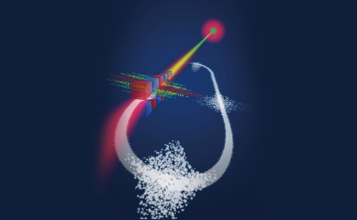
Currently we produce EUV by spinning a disk of molten tin, then shooting the droplets with a laser to disperse them, then shooting them with a bigger laser to ionize them and emit EUV in all directions, which is then focused to a point via a dozen ultra precise lenses and mirrors.
This is an extremely finicky process and some fabs never get quite efficient enough to break even. When they do, nothing is changed, including the color of the paint of the room the fab is in.
Play stupid games…
This will be an incredible development when they pull it off. It seems murky to me how semiconductor shrinks will be pulled of after the next few, but this could really change things.
I expect that the next big development is going to be using alternative substrates that have different physical properties from silicon. For example, Chinese researchers recently showed that they can produce a 12 inch wafer using a 2d material. At this point it’s really a question of how long it’s going to iron out the process to put it into mass production. Chips made using alternate substrates have the potential of making silicon look like vacuum tubes.
I dub thee the base cannon.


